























An ambitious chip startup that spent over seven years quietly redesigning computer memory architecture has emerged from stealth mode, believing its novel approach can help alleviate the global memory chip shortage, provided the technology can be scaled successfully.
Kepler Computing and Its New Memory Architecture
Founded in 2018 by a team of physicists and computer scientists in San Jose, California, Kepler Computing states that it has developed a fresh architecture for high-bandwidth memory that directly tackles supply bottlenecks constraining the computing market. While traditional chipmakers rely heavily on expensive extreme ultraviolet lithography to shrink transistors and pack more technology into limited space, Kepler claims its three-dimensional stacking approach and proprietary material increase density without any reliance on EUV, while remaining compatible with existing semiconductor fabrication plants.
SRAM and HBM Developed in Parallel
The company reports achieving similar gains for the high-speed cache memory typically integrated into CPUs, GPUs, and XPUs. This SRAM sits inside the core of a chip die to reduce data transfer times, whereas HBM utilizes stacks of separate DRAM components. Debo Olaosebikan, cofounder and chief executive officer of Kepler, noted that while the initial plan focused on SRAM before moving to DRAM and HBM, the explosive demand following the launch of ChatGPT in 2022 pushed the team to develop their HBM roadmap in parallel.
Substantial Funding and Backing from Industry Giants
Over the past few years, the firm has raised $468 million in funding from prominent backers including GlobalFoundries, Intel Capital, AMD Ventures, British investment fund Baillie Gifford, and Bill Gates through his private Gates Frontier fund. Additionally, the US Department of Commerce committed up to $245 million in July to help Kepler develop a new class of high-performance AI memory technology enabled by advanced 3D and ferroelectric innovations.
Testing Facilities in Singapore and Vermont
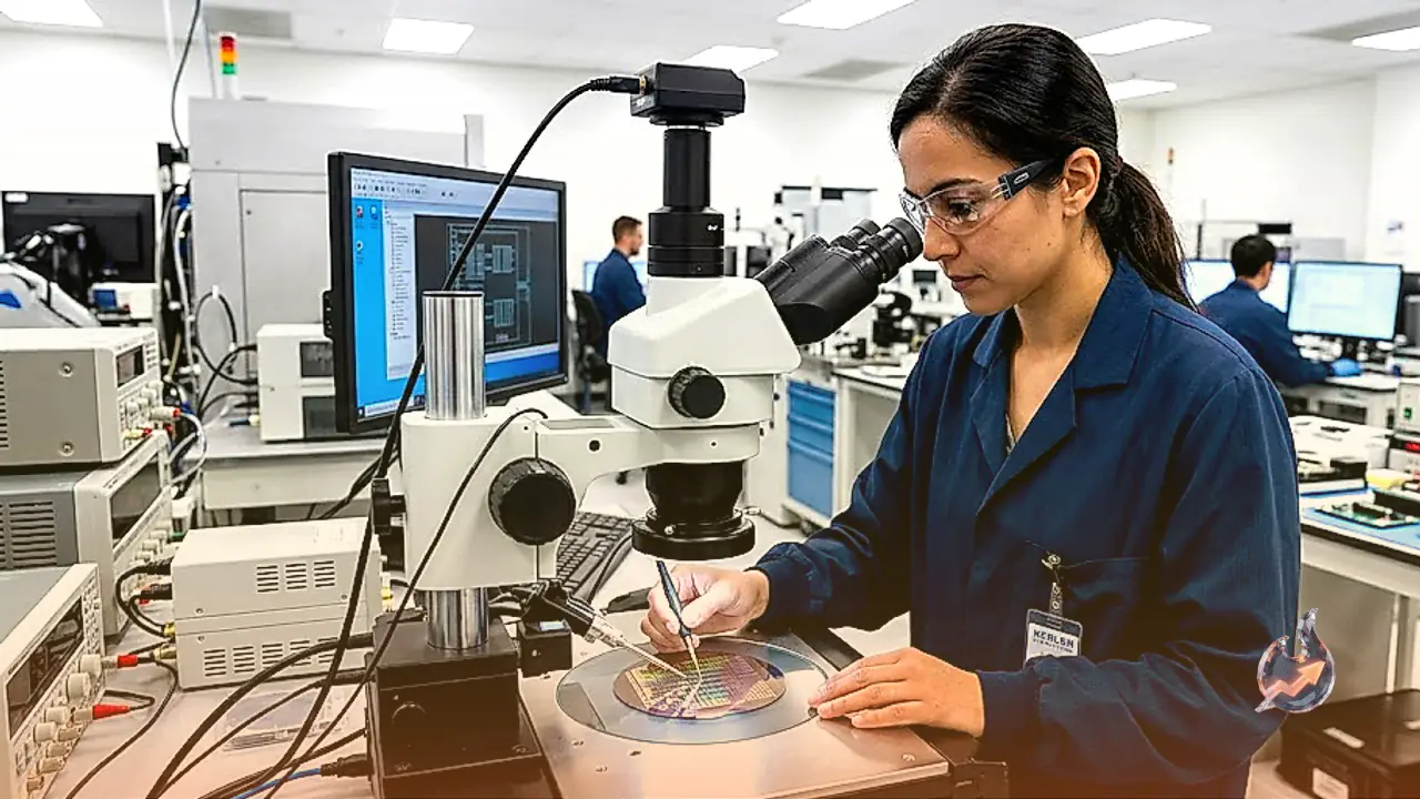
Much of Kepler's current testing takes place in Singapore at a facility operated by GlobalFoundries, which also serves as a manufacturing partner and a $50 million investor. Over the past two years, Kepler has established mini-fabs to produce memory chips alongside GlobalFoundries' 28-nanometer chips, while also running tests in Burlington, Vermont.
Industry Demands and the Need for New Approaches
Investors and company executives argue that this new memory-building method arrives at an opportune moment. The global memory chip shortage has reaffirmed the exorbitant cost and painstaking nature of building new fabs, alongside the cyclical demands of specific memory types. In an artificial intelligence-driven world, HBM has become the premier memory choice, prompting major makers like SK Hynix and Micron to invest billions in new fabs.
Srini Ananth, managing director at Intel Capital, remarked that the market dictates the demand for both SRAM and HBM, validating the company's dual-path approach.
Bypassing EUV with Ferroelectric Materials
By bypassing ultraviolet lithography, Kepler joins a select group of startups working around major semiconductor manufacturing bottlenecks. The firm claims it can produce SRAM matching the density of 2-nanometer or 3-nanometer chips without investing in EUV equipment. Ed Kaste, senior vice president of GlobalFoundries' CMOS business, praised the approach for offering a new material system with multigenerational scaling potential without requiring entirely new fab systems.
Kepler's strategy focuses on increasing memory supply within existing fabs rather than waiting for new facilities to be built. The dual-pronged approach involves a novel 3D-manufacturing technique for HBM that fits more chips within a fixed footprint, alongside improved SRAM density using ferroelectrics that read and write data at lower voltages. CTO Sasi Manipatruni noted that the team went through 35 composite iterations before finding the ideal material class.
Production Roadmap and Scaling Challenges
During early builds with GlobalFoundries, Kepler converted a standard fab into a next-generation facility in just eight months, compared to the typical 24-month timeframe. The company plans to ship its first HBM samples later this year, ramp up Singapore production next year, and initiate US chip production in 2028.
While Kaste expressed confidence in these fundamental breakthroughs, he cautioned that introducing iron into the composite material requires strict isolation to prevent facility contamination. Austin Lyons, a chip analyst for Creative Strategies, emphasized that overcoming contamination and tooling limitations to achieve cost-effective scale remains the ultimate test for any manufacturing innovation.