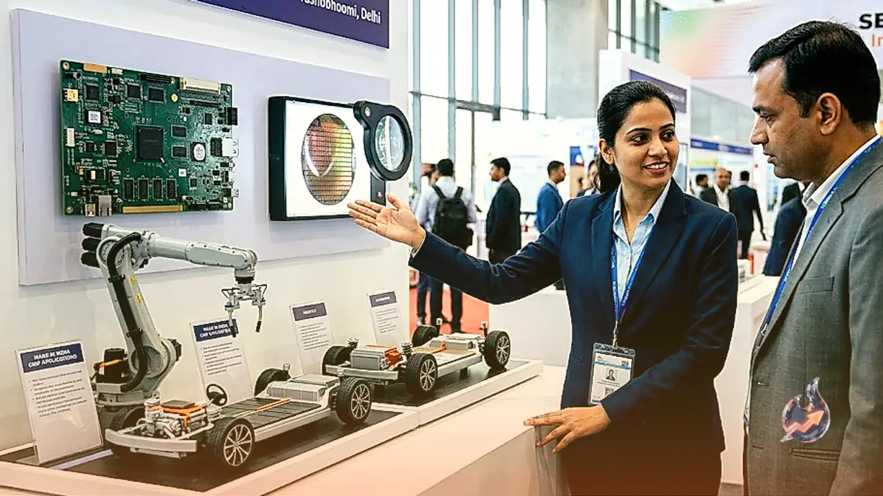
























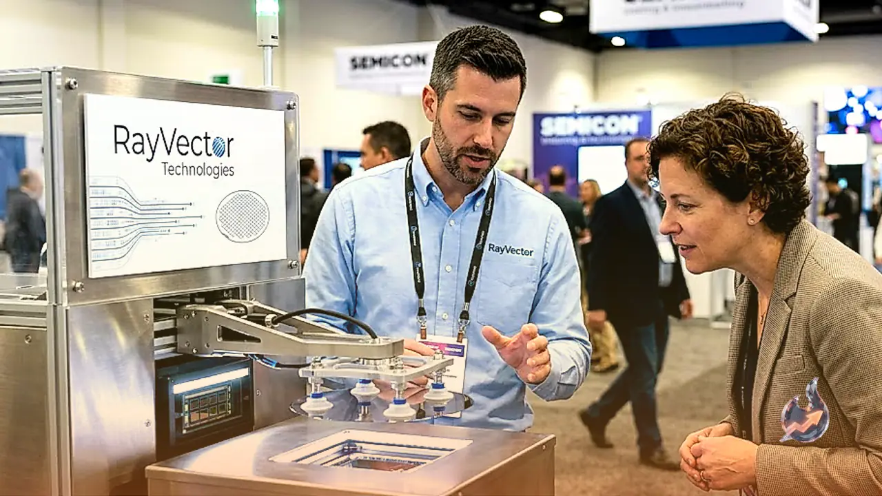

In the extraordinarily demanding environment of semiconductor manufacturing, even an invisible mechanical defect can trigger catastrophic downtime for an entire fabrication facility. Showcasing indigenous innovation at SEMICON, Indian deep-tech venture RayVector Technologies unveiled its advanced wafer handling system. Powered by an integrated multi-sensor module, the equipment is engineered to deliver continuous monitoring and swift fault identification during the most critical phases of silicon processing.
The Critical Role Of Wafers And High Risks In Fabrication
The foundation of every microchip begins with the silicon wafer, a high-precision circular disk upon which thousands of microscopic integrated circuits are layered. Explaining the sensitivity of the process, RayVector Technologies Chief Technology Officer Chakravarthi Elumalai pointed out that wafers represent the single most vital component in semiconductor production. Commercial wafers carry starting price tags of approximately $2,000, quickly climbing into many thousands of dollars depending on architectural complexity.
Subjecting such expensive materials to multi-stage fabrication means that unspotted microscopic defects carry enormous financial peril. If flaws slip through undetected during early handling, the subsequent processing ruin reaches immense proportions. RayVector claims its specialized sensor framework detects even the slightest physical anomalies in real time, delivering early alerts that allow operators to intervene before compounded damage occurs.
Preventing Multi-Million-Dollar Shutdowns And Production Bottlenecks
Semiconductor fabrication facilities operate continuously around the clock, relying on uninterrupted material flow. When a major handling defect or mechanical error goes unnoticed on the assembly line, operators often have no choice but to halt the entire manufacturing plant. Resolving the root issue and recalibrating the cleanroom environment can stall output for several consecutive days, causing monetary damage running into millions of dollars. Through precision tracking, this compact sensor module serves as an indispensable fail-safe, shielding chipmakers from potentially disastrous financial losses.
Global Giants Adopt The Tech As India Expands Beyond Basic Manufacturing
The practical necessity of such precision tools is underscored by their reception among top-tier global manufacturers. Chakravarthi Elumalai revealed that semiconductor powerhouses such as Samsung, Intel, and TSMC have integrated RayVector's technology into their operations. This adoption demonstrates that Indian technological capability extends far beyond basic device assembly into sophisticated core engineering.
India's overarching semiconductor roadmap is deliberately moving beyond the establishment of physical factories to foster an exhaustive domestic ecosystem. This strategy links chip architecture design, advanced sensory equipment, imaging technologies, artificial intelligence integration, precision testing, hardware fabrication tools, and specialized software. Reflecting this broader mission, Prime Minister Narendra Modi reiterated during his address that the country aims to nurture fabless enterprises and generate domestic semiconductor intellectual property, while intensifying development in compound semiconductors, silicon photonics, and dedicated AI chips.
The AI Revolution Accelerates Specialized Chip Requirements
The rapid proliferation of artificial intelligence systems is reshaping hardware demands across the globe. Modern AI data hubs require thousands of high-performance microprocessors functioning synchronously to manage expansive workloads. As society integrates advanced algorithmic processing deeper into everyday infrastructure, computing requirements surge proportionally, necessitating larger numbers of chips, broader data throughput, and massive electricity supplies.
Consequently, the race among semiconductor developers is no longer solely about shrinking transistors or accelerating clock speeds. The industry faces difficult technical hurdles around placing memory physically closer to compute units, coordinating multi-chip packaging, achieving instantaneous data transfers, and effectively managing severe thermal output alongside steep power consumption.
Empowering A Skilled Engineering Generation For Deep-Tech Leadership
Amid this global technological recalibration, India's most significant competitive advantage lies in its vast pool of engineering talent. Addressing the workforce demand, Prime Minister Narendra Modi shared that the government established a concrete target to train 100,000 engineering students explicitly for the semiconductor sector. More than 70,000 young professionals have already completed specialized training under this national initiative.
These numbers highlight a targeted strategy: India is not simply laying the groundwork for cleanrooms and physical assembly lines, but is actively cultivating the research talent required to architect, refine, and pioneer the next generation of semiconductor technologies on the global stage.